Explanation of Crystal Units
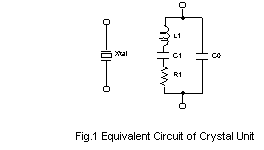
1 Equivalent Circuit
Vibration of a crystal unit is actually mechanical vibration. However, the crystal unit can be expressed by a two terminal network if its behavior is electrically converted. The series circuit consisting of L1, C1, and R1 is related to elastic vibration, while the element C0 connected in parallel to the series arm as a capacitance attributable to the dielectric body of a quartz crystal plate. The resistance R1 is a resonance resistance of the crystal unit at the series resonance frequency. (See Fig.1.)
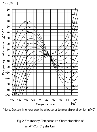
2 Frequency-Temperature
Characteristics of an AT-cut The frequency-temperature characteristics of an AT-cut crystal unit most generally used at present are expressed by cubic curves. (See Fig.2.) A crystal plate is cut at an angle at which a required frequency tolerance is obtained in the given operating temperature range. Actually, however there can be some dispersion in apparent cutting angle due to the result of cutting and polishing accuracy in the successive processes. Therefore, it is necessary to raise processing accuracy.
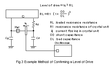
3 Level of Drive
Since a crystal unit performs mechanical vibration, too much vibration may lead to unstable oscillation frequency, and finally to destruction in the worst case. When designing an oscillation circuit, the level of drive should be examined so as to use an oscillator below the level specified by our company. Fig.3 shows an example method of confirming a level of drive. The method employs a current probe to measure the crystal oscillator current. In this case the level of drive is as follows:
4 Load Capacitance
The load capacitance CL is a factor for determining the "conditions" of a crystal unit when used in the oscillation circuit. In an ordinary oscillation circuit, the crystal unit is used in a range where it functions as an inductive reactance. In such usage, the oscillation circuit operates as a capacitive reactance. In other words, when the oscillation circuit is seen from both terminals of the crystal unit, the oscillation circuit can be expressed as a series circuit of a negative resistance -R and a capacitance CL. At that time this capacitance is called the load capacitance. The relationship between load capacitance and oscillation frequency is not linear. When the load capacitance is small, the amount of frequency variation is large, and when the load capacitance is increased, frequency variation lowers. If the load capacitance is lessened in the oscillation circuit to secure a large allowance for the oscillation frequency, the frequency stability will be greatly influenced even by a small change in the circuit. The load capacitance can be any values, but 10~30pF is better.
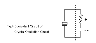
5 Equivalent Circuit of Crystal Oscillation Circuit
When a crystal unit is actuated as an inductive reactance in an oscillation circuit, the relationship between crystal unit and oscillation circuit is shown in Fig.4. To improve the starting conditions of the oscillation circuit, it is preferable to increase the value of negative resistance -R which parameter of the oscillation circuit. The starting conditions will become worse if a circuit without much allowance in negative resistance (less negative resistance) is combined with a crystal unit having a larger resonance resistance. The oscillation circuit should be designed to a goal such that the value of negative resistance is 5 to 10 times the resonance resistance. It is also necessary that the center value of load capacitance (to determine the absolute value of oscillation frequency) and the variable range (fine adjustment range of oscillation frequency) are maintained at the optimum values in the oscillation circuit.
6 Oscillation circuit
A typical oscillation circuit composed of a crystal unit is introduced below. Element constants used are for example.
(1) Crystal units are designed to have lower limitable level of drive, of 100µW and below. Prior to use, the crystal current should be examined in an actually mounting circuit. (See Fig.3.)
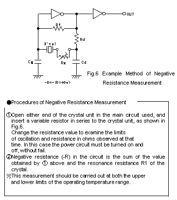
(2) The negative resistance of a circuit must be checked. Confirmation of negative resistance is possible according to Fig.6. A goal of negative resistance is designed to 5 or more times of the resonance resistance.
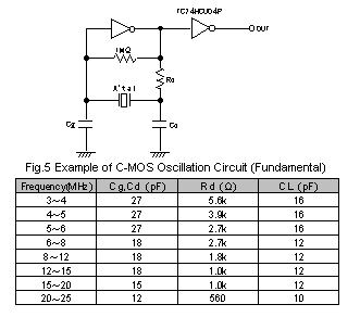
(3) The Rd in the circuit diagram is indispensable when used in a C-MOS oscillation circuit. (See Fig.5.) If this Rd is attached, the level of drive is kept within the specified value and stable oscillation frequency can be obtained.
(4) Cg and Cd should be used within the range of 10 ? 30 pF. If Cg and Cd are used below 10 pF or above 30 pF, oscillation may be easily affected by circuit performance, level of drive may increase, or negative resistance may decrease, thus failing in maintaining stable oscillation.
(5) The layout for crystal oscillation circuits should be arranged as short as possible. The stray capacitance between circuits and ground patterns should be reduced. Crossing of crystal oscillation circuits patterns over other circuit patterns should be avoided.
(6) If the circuits used, IC types, and IC manufacturers are different, frequency, level of drive, and negative resistance should be confirmed.
* Overtone oscillation circuits need additional consultation
7 Notes for Crystal Unit Applications
(1) It has the possibility that a crystal element fractures when an excessive shock and a vibration more than the regulation are added at the time of the conveyance or circuit board mounting. Be sure to do characteristic confirmation when a shock more than the regulation, a vibration are added.
(2) Ultrasonic-wave cleaning may cause deterioration of crystal units.
(3) Leave it and bend 0.5 or more mm from the foundation of the lead in the case of lead type.
(4) The deformation of the extreme circuit board sometimes brings about a pattern comes off, a terminal and electrode comes off, a crack in the solder. Be careful when you install it in the position where the curve of the circuit board appears greatly when you divide a circuit board after you mount it specially.
(5) Select the model whose shock is small as much as possible, and use it after confirmation in advance when you use an automatic loading machine.
(6) Compared with the lineups of JC-49/U, small crystal units ( HC-49U/S, HC-49USM, UM-1, SMD) are designed to have lower limitable level of drive, of 100µw and below. Prior to use, therefore the crystal current should be examined in an actually mounting circuit.
(7) The negative resistance of a circuit must be checked. Confirmation of negative resistance is possible according to Fig.6, goal of negative resistance is about 5 times of the resonance resistance.
(8) The Rd in the circuit diagram is indispensable when used in a C-MOS oscillation ciucuit (see Fig.5.). If this Rd is attahcedm the level of drive is kept within the specified value and stable oscillation frequency can be obtained.
(10) Cg and Cd should be used within the range of 10~30pF, if Cg and Cd are used below 10pF or above 20pF oscilltion may be easily affected by circuit performance, level of drive may increase, or negative resistace may decrease, thus failing in maintaining stable oscillation.
(11) The layout for crystal oscillation circuits should be arranged as short as possible.
(12) The stray capacitance between circuits and ground patterns should be reduced.
(13) Crossing of crystal oscillation ciucuit patterns over other circuit patterns should be avoided.
(14) If the circuit used are IC types, and IC manufacturers are different, Frequency, Level of Drive, and Negative Resistance should be confirmed.
(15) Overone oscillation circuits need additional consulation.